7*24小时服务热线:
13724329562


5V 12V可选
DESCRIPTION
PD (Powered Device) Integrated Module (Isolation Type)
FEATURES
Fully IEEE 802.3af compliant
12.95 watt output load
IEEE Power class programmable (Green)
1500 Volt DC isolation (Input to Output)
5V, 12V,24VDC output voltage models
Compact package minimum PCB footprint
Minimal external components required
Overload and short circuit protection
Wide input voltage (36V to 57V DC)
Adjustable output voltage
Support PoE applications in both of Fast / Gigabit Ethernet environments.
Low output ripple and noise
Low cost
APPLICATION AREAS
Security and alarm systems
Voice over IP phones
Access control systems
IP Cameras
Displays, Net Monitors
Public address systems
Wireless access points
Environmental control
Telemetry
Remote environmental monitoring
1 Product Overview
1.1 DP9900 Product Selector
|
Part Number |
Nominal OutputVoltage
|
Output Power | |
|
70˚C |
85˚C | ||
|
DP9905M |
5.0V |
9 Watts |
6 Watts |
|
DP9912M |
12.0V |
12 Watts |
9 Watts |
|
DP9924M |
24.0V |
12 Watts |
11 Watts |
|
DP9905LP |
5.0V |
7 Watts |
4.5 Watts |
|
DP9912LP |
12.0V |
10 Watts |
6 Watts |

1.2Pin Description
|
Pin # |
Name |
Description |
|
1 |
+VDC |
DC Output.This pin provides the regulated output from the DC/DC converter. |
|
2 | ||
|
3 |
-VDC |
DC Return.This pin is the return path for the +VDC output. |
|
4 |
ADJ |
Output Adjust.The output voltage can be adjusted from is nominal value, by connecting an external resistor from this pin to either the +VDC pin or the -VDC pin. |
|
5 |
VIN+ |
Direct Input +. This pin connects to the positive (+) output of the input bridge rectifiers. |
|
6 | ||
|
7 |
VIN- |
Direct Input -. This pin connects to the negative (-) output of the input bridge rectifiers. |
|
8 |
Table 2: Pin Description
2 Functional Description
2.1Typical Connections
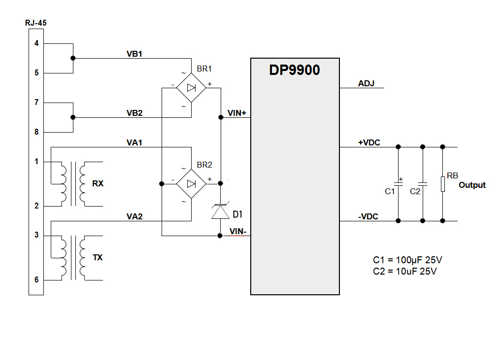
Figure 3: Typical Connection Diagram
BR1,BR2=MB6S;D1=SMAJ58A;RB= ≥ I Load min
2.2 Output Voltage Adjustment
The DP9900 series has an OADJ pin, which allows the output voltage to be increased or decreased.
Figure4 shows how the ADJ pin is connected.

Figure4: Output Adjustment
|
Reducing the output voltage, connect R between ADJ and +VDC | |||
|
Value of R |
DP9905 output |
DP9912 Output |
DP9924 Output |
|
Open Circuit |
5.00V |
12.07V |
23.93V |
|
0 Ohms |
4.48V |
10.0V |
19.85V |
|
100K |
4.76V |
11.15V |
21.85V |
|
470k |
4.92V |
11.76V |
23.23V |
|
| |||
|
Increasing the output voltage, connect R between ADJ and -VDC | |||
|
Value of R |
DP9905 output |
DP9912 output |
DP9924 Output |
|
Open Circuit |
5.00V |
12.07V |
23.93V |
|
0 Ohms |
5.66V |
12.75V |
24.6V |
|
100K |
5.27V |
12.34V |
24.2V |
|
470k |
5.08V |
12.16V |
24.01V |
Table 3: Output Adjustment Resistor (R) Value
3 Electrical Characteristics
3.1Absolute Maximum Ratings
|
|
Parameter |
Symbol |
Min |
Max |
Units |
|
1 |
DC Supply Voltage |
VCC |
-0.3 |
60 |
V |
|
2 |
DC Supply Voltage Surge for 1ms |
VSURGE |
-0.6 |
80 |
V |
|
3 |
Storage Temperature |
TS |
-40 |
+100 |
˚C |
3.2Recommended Operating Conditions
|
|
Parameter |
Min |
Typ |
Max |
Units |
|
1 |
Input Supply Voltage |
36 |
48 |
57 |
V |
|
2 |
Under Voltage Lockout |
30 |
|
36 |
V |
|
3 |
Input Curren |
|
350 |
400 |
mA |
|
4 |
Operating Temperature |
-40 |
25 |
85 |
℃ |
|
5 |
IEEE 802.3af |
Class 0 | |||
3.3DC Electrical Characteristics
|
|
DC Characteristic |
Variant |
Sym |
Min |
Typ1 |
Max |
Units |
|
1 |
Nominal Output Voltage |
DP9924 |
+VDC |
23.5 |
24 |
24.5 |
V |
|
DP9912 |
11.6 |
12 |
12.4 | ||||
|
DP9905 |
4.75 |
5 |
5.25 | ||||
|
2 |
Minimum Load2 |
DP9924 |
ILOAD |
20 |
|
|
mA |
|
DP9912 |
40 | ||||||
|
DP9905 |
100 | ||||||
|
|
DC Characteristic |
Variant |
Sym |
Min |
Typ1 |
Max |
Units |
|
3 |
Output Current (VIN = 48V) |
DP9924M |
Iout |
|
0.5 |
|
A |
|
DP9912M |
1.0 | ||||||
|
DP9912LP |
0.8 | ||||||
|
DP9905M |
1.8 | ||||||
|
DP9905LP |
1.4 |
|
4 |
Line Regulation |
DP9924 |
VLINE |
|
0.15 |
|
% |
|
DP9912 |
0.05 | ||||||
|
DP9905 |
0.05 | ||||||
|
5 |
Load Regulation – Min to Max (VIN = 48V) |
DP9924 |
VLOAD |
|
0.15 |
|
% |
|
DP9912 |
0.1 | ||||||
|
DP9905 |
0.1 | ||||||
|
6 |
Output Ripple and Noise5@ Max load |
DP9924M |
VRN |
|
TBD |
|
mVp-p |
|
DP9912M |
146mV | ||||||
|
DP9912LP |
198mV | ||||||
|
DP9905M |
124mV | ||||||
|
DP9905LP |
TBD | ||||||
|
7 |
Peak Efficiency |
DP9924M |
EFF |
|
87 |
|
% |
|
DP9912M | |||||||
|
DP9912LP |
86 | ||||||
|
DP9905M |
83 | ||||||
|
DP9905LP | |||||||
|
8 |
Short-Circuit Duration3 |
|
TSC |
|
|
∞ |
sec |
|
9 |
Isolation Voltage (I/O) - Impulse Test |
|
VISO |
|
|
1500 |
VPK |
Note 1: Typical figures are at 25°C with a nominal 48V supply and are for design aid only. Not Guaranteed
Note 2: The module can emit an audible noise, if operated at less than the stated minimum ILOAD and cause the PSE to fail its MPS.
Note 3: >200mohm short due to thermal limitation.
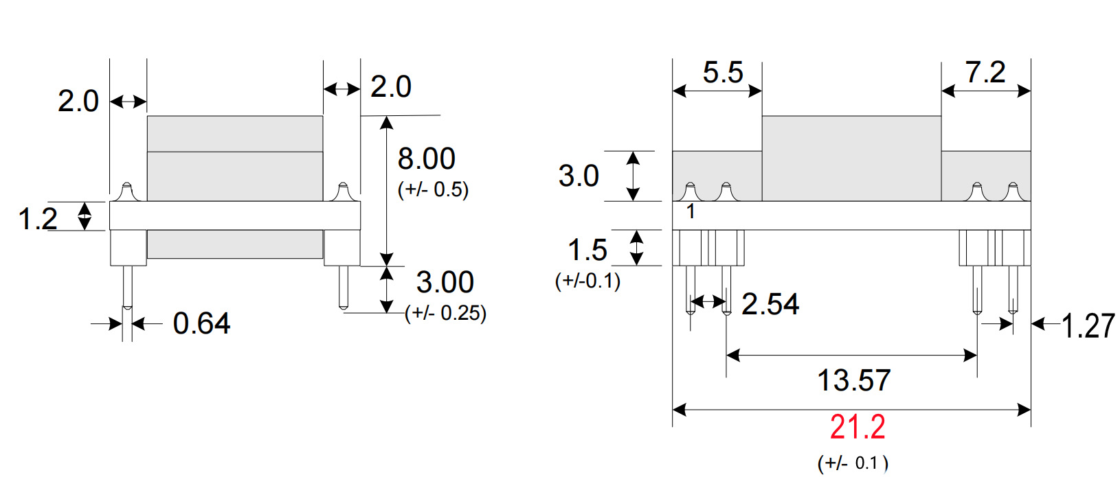
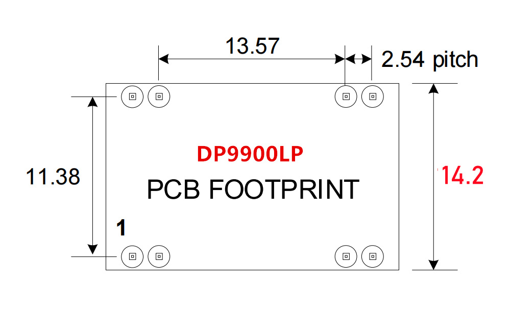
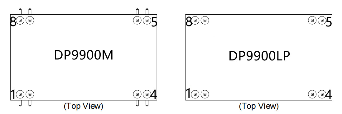
4 PackDPe
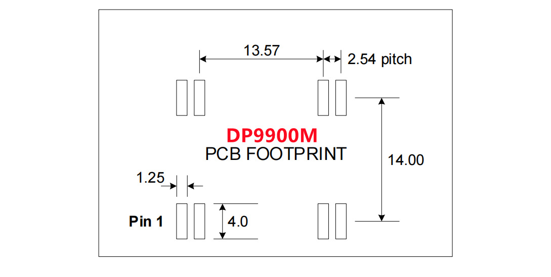
4.1 DP9900M


4.2 DP9900LP